
Band 10
Introduction to VLSI Silicon Devices Physics, Technology and Characterization
-
- Hardcover ausgewählt
- Taschenbuch
- eBook
-
Sprache:Englisch
Fr. 191.00
inkl. gesetzl. MwSt.,
Beschreibung
Produktdetails
Einband
Gebundene Ausgabe
Erscheinungsdatum
31.12.1985
Verlag
Springer UsSeitenzahl
570
Maße (L/B/H)
23.4/15.6/3.3 cm
Gewicht
1007 g
Auflage
1986
Sprache
Englisch
ISBN
978-0-89838-210-5
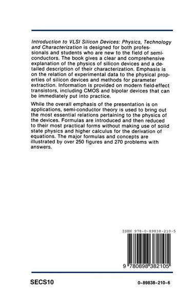
There was a long felt need for this book in industrial and academic institutions. It provides new engineers, as well as practicing engineers and advanced laboratory personnel in the field of semiconductors a clear and thorough discussion of state-of-the-art silicon devices, without resorting to the complexity of higher mathematics and physics. This difficult task was made possible by detailing the explanation of equations that describe the device operation and characteristics without endeavoring their full derivation. This is reinforced by several problems which reflect practical cases observed in the laboratory. The problems are given after introducing a major equation or concept. They are arranged in the order of the text rather than in the order of difficulty. The answers to most of the problems are given in order to enable the student to "self-check" the method used for the solutions. The illustrations may prove to be of great help to "newcomers" when dealing with the characterization of real devices and relating the measured data to device physics and process parameters. The new engineer will find the book equivalent to "on the job training" and acquire a working knowledge of the fundamental principles underlying silicon devices. For the engineer with theoretical background, it offers a means for direct application of solid state theory to device analysis and synthesis. The book originated from a set of notes developed for an in-house one-year course in Device Physics, Technology and Characterization at IBM.
Noch keine Bewertungen vorhanden
Verfassen Sie die erste Bewertung zu diesem Artikel
Helfen Sie anderen Kundinnen und Kunden durch Ihre Meinung.