
Band 9
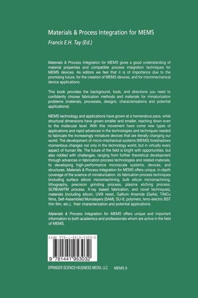
Materials & Process Integration for MEMS
Aus der Reihe
Microsystems
-
- Hardcover
- Taschenbuch ausgewählt
- eBook
-
Sprache:Englisch
Fr. 192.00
inkl. gesetzl. MwSt.,
Beschreibung
Produktdetails
Einband
Taschenbuch
Erscheinungsdatum
03.12.2010
Herausgeber
Francis E. H. TayVerlag
Springer UsSeitenzahl
299
Maße (L/B/H)
23.5/15.5/1.8 cm
Gewicht
499 g
Auflage
Softcover reprint of hardcover 1st edition 2002
Sprache
Englisch
ISBN
978-1-4419-5303-2
The field of materials and process integration for MEMS research has an extensive past as well as a long and promising future. Researchers, academicians and engineers from around the world are increasingly devoting their efforts on the materials and process integration issues and opportunities in MEMS devices. These efforts are crucial to sustain the long-term growth of the MEMS field. The commercial MEMS community is heavily driven by the push for profitable and sustainable products. In the course of establishing high volume and low-cost production processes, the critical importance of materials properties, behaviors, reliability, reproducibility, and predictability, as well as process integration of compatible materials systems become apparent. Although standard IC fabrication steps, particularly lithographic techniques, are leveraged heavily in the creation of MEMS devices, additional customized and novel micromachining techniques are needed to develop sophisticated MEMS structures. One of the most common techniques is bulk micromachining, by which micromechanical structures are created by etching into the bulk of the substrates with either anisotropic etching with strong alk:ali solution or deep reactive-ion etching (DRIB). The second common technique is surface micromachining, by which planar microstructures are created by sequential deposition and etching of thin films on the surface of the substrate, followed by a fmal removal of sacrificial layers to release suspended structures. Other techniques include deep lithography and plating to create metal structures with high aspect ratios (LIGA), micro electrodischarge machining (J.
Noch keine Bewertungen vorhanden
Verfassen Sie die erste Bewertung zu diesem Artikel
Helfen Sie anderen Kundinnen und Kunden durch Ihre Meinung.