• Produktbild: Very Large Scale Integration (VLSI)
  • Produktbild: Very Large Scale Integration (VLSI)
Band 5

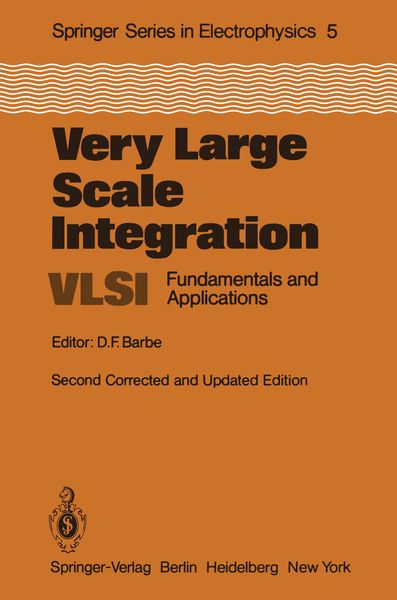
Very Large Scale Integration (VLSI) Fundamentals and Applications

Fr. 137.00

inkl. gesetzl. MwSt., Versandkostenfrei


Beschreibung

Produktdetails

Einband

Taschenbuch

Erscheinungsdatum

22.04.2012

Herausgeber

D.F. Barbe

Verlag

Springer Berlin

Seitenzahl

304

Maße (L/B/H)

23.5/15.5/1.8 cm

Gewicht

487 g

Auflage

Second Edition 1982

Sprache

Englisch

ISBN

978-3-642-88642-3

Beschreibung

Produktdetails

Einband

Taschenbuch

Erscheinungsdatum

22.04.2012

Herausgeber

D.F. Barbe

Verlag

Springer Berlin

Seitenzahl

304

Maße (L/B/H)

23.5/15.5/1.8 cm

Gewicht

487 g

Auflage

Second Edition 1982

Sprache

Englisch

ISBN

978-3-642-88642-3

Herstelleradresse

Springer-Verlag KG
Sachsenplatz 4-6
1201 Wien
AT

Email: GPSR Kontakt

Noch keine Bewertungen vorhanden

Verfassen Sie die erste Bewertung zu diesem Artikel

Helfen Sie anderen Kundinnen und Kunden durch Ihre Meinung.

Kundinnen und Kunden meinen

Bewertungen (0)

  • Produktbild: Very Large Scale Integration (VLSI)
  • Produktbild: Very Large Scale Integration (VLSI)
  • 1. Introduction.- 1.1 Outlook.- 1.2 Scope of this Volume.- 1.3 Summary.- References.- 2. VLSI Device Fundamentals.- 2.1 Fundamentals of VLSI Device Improvements.- 2.1.1 Relative Importance of Chip Area, Circuit Innovation, and Minimum Dimension.- 2.1.2 Device Scaling Fundamentals.- 2.2 Problem Areas for VLSIC’s.- 2.2.1 Interconnections.- 2.2.2 Ionizing Particle Effects on Dynamic Logic Circuits.- 2.2.3 Active Scaling Parasitics.- 2.3 Small-Geometry MOS Anomalies.- 2.3.1 Short Channel Vt Effect.- 2.3.2 Narrow Width Vt Effect.- 2.3.3 Combination Narrow Width/Short Channel (Minimum Size) Vt Effect.- 2.3.4 Short Channel Limit for Subthreshold Conduction Effects.- 2.4 VLSIC Projections.- 2.5 Conclusions.- References.- 3. Advanced Lithography.- 3.1 Optical Lithography.- 3.1.1 Optical Resists.- 3.1.2 Contact and Proximity Printing.- 3.1.3 Projection Printing.- 3.2 Electron Lithography.- 3.2.1 Resists.- 3.2.2 Mask Generation.- 3.2.3 Electron Optics.- 3.2.4 Vector Scan.- 3.2.5 Raster Scan.- 3.2.6 Variable Beam Shape.- 3.2.7 Electron Projection.- 3.3 X-Ray Lithography.- 3.3.1 Resists.- 3.3.2 Proximity Printing.- 3.3.3 X-Ray Sources.- 3.3.4 Masks.- 3.3.5 Synchrotron Radiation.- 3.4 Ion Lithography.- 3.5 Conclusion.- References.- 4. Computer Aided Design for VLSI.- 4.1 What is Computer Aided Design?.- 4.2 History.- 4.3 State-of-the-Art.- 4.3.1 Specification.- 4.3.2 Synthesis.- 4.3.3 Simulation.- 4.3.4 Testability.- 4.3.5 Partitioning.- 4.3.6 Layout.- 4.3.7 Topological Analysis.- 4.3.8 Timing Analysis.- 4.3.9 Documentation.- 4.3.10 Data Management.- 4.3.11 Summary of Current Use of CAD.- 4.4 Perspective.- 4.4.1 The Connectivity Problem.- 4.4.2 The Layout Problem.- 4.4.3 The Problem with Mistakes.- 4.5 Management of Complexity.- 4.6 Structured Design.- 4.7 Functional Design Tools.- 4.7.1 Specification.- 4.7.2 Synthesis.- 4.7.3 Simulation.- 4.7.4 Test Development.- 4.7.5 Physical Constraints on the Functional Design.- 4.8 Physical Design Tools.- 4.8.1 Partitioning.- 4.8.2 Physical Layout.- 4.8.3 Topological Analysis.- 4.8.4 Timing Analysis.- 4.9 Design Management.- 4.9.1 Data Base.- 4.9.2 Data Management System.- 4.9.3 Data Configuration Management.- 4.9.4 Product Development Plan.- 4.9.5 Management Information System.- 4.10 Conclusion.- References.- 5. GaAs Digital Integrated Circuits for Ultra High Speed LSI/VLSI.- 5.1 Performance Advantages Expected for GaAs ICs.- 5.2 Circuit Approaches for GaAs Digital Logic ICs.- 5.2.1 Enhancement Mode FET Logic Approaches.- 5.2.2 Single Supply Enhancement — Depletion Mode MESFET Logic.- 5.2.3 D-MESFET Approach/Buffered FET Logic.- 5.2.4 D-MESFET Schottky Diode-FET Logic (SDFL).- 5.2.5 Transferred Electron Logic Device (TELD) Approach.- 5.3 GaAs Integrated Circuits: Fabrication Technology.- 5.3.1 Evolution of GaAs Process Technology.- 5.3.2 Mesa Implanted D-MESFET.- 5.3.3 Mesa Epitaxial/Implanted E-MESFET.- 5.3.4 Self-Aligned Epitaxial D-MESFET.- 5.3.5 Planar Implanted E-JFET.- 5.3.6 Planar Implanted D-MESFET.- 5.3.7 Fabrication Technology Review: Conclusions.- 5.3.8 Planar VLSI Compatible Fabrication Technology.- 5.4 Performance Results for GaAs Digital ICs.- 5.5 Summary, Conclusions and Projections.- Appendix: Nonlinear Switching Analysis for PD?d.- Dependence on ?d and FET K-Value.- References.- 6. VLSI Architecture.- 6.1 VLSI Technology Basis.- 6.2 VLSI Device Architecture.- 6.2.1 Device Architecture Issues.- 6.2.2 VLSI Device Design Example.- 6.2.3 Example VLSI Designs.- 6.3 VLSI System Architecture.- 6.3.1 Signal Processing Algorithms.- 6.3.2 Signal Processing Architectures.- 6.3.3 Implementation.- 6.3.4 Adaptive Sonar Equalizer Design Example.- 6.4 VLSI Architecture Case Study.- 6.4.1 Basic Concepts.- 6.4.2 DBF Emulation Model.- 6.4.3 VLSI for the Real-Time DBF System.- 6.5 Conclusion.- References.- 7. VLSI Applications and Testing.- 7.1 VLSI Applications.- 7.1.1 Telephone Echo Canceller.- 7.1.2 Narrow Band Voice Channel Processing.- 7.1.3 Dual Tone Multifrequency (DTMF) Receiver.- 7.1.4 TDM-FDM Transmultiplexer.- 7.1.5 Synthetic Aperture Radar (SAR).- 7.1.6 VLSI Memories.- 7.2 VLSI Testing.- 7.2.1 Design for Testing.- 7.3 Conclusion.- References.- 8. VHSIC Technology and Systems.- 8.1 IC Progress.- 8.2 Throughput Capacity.- 8.3 Defense Systems.- 8.4 The VHSIC Program.- 8.4.1 Approach.- 8.4.2 Schedule.- 8.5 Example Brassboard Systems.- 8.5.1 Command, Control and Communications.- 8.5.2 Radar.- 8.5.3 Electronic Warfare.- 8.5.4 Image Processing.- 8.5.5 General-Purpose Computers.- 8.6 Scaling to Smaller Dimensions: Benefits and Barriers.- 8.6.1 Benefits.- 8.6.2 Negative Effects.- 8.6.3 Noise Margins.- 8.6.4 Electromagnetic Interference.- 8.6.5 Soft Errors.- 8.6.6 Radiation Hardness.- 8.6.7 Economical Lithography.- 8.7 Computer-Aided Design.- 8.7.1 The Increasing Design Problem.- 8.7.2 The Macrocell Approach.- 8.8 Testing.- 8.9 Substrates.- 8.10 Summary.- References.- 9. VLSI in Other Countries.- 9.1 Past Major Semi conductor Programs.- 9.1.1 Past Developments in The United States.- 9.1.2 Past Developments in Japan.- 9.2 Present National Semiconductor Programs.- 9.2.1 United Kingdom.- 9.2.2 France.- 9.2.3 Federal Republic of Germany.- 9.2.4 Italy.- 9.2.5 The Netherlands.- 9.2.6 Japan.- 9.2.7 Korea.- 9.3 Future Prospects.- References.- Additional References.- Additional References.