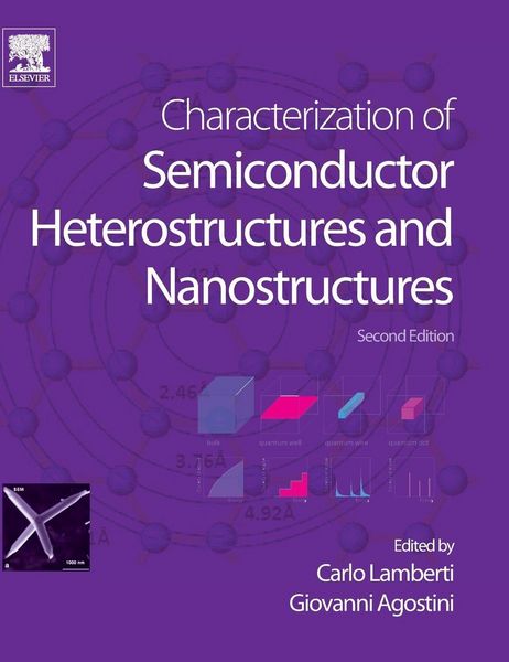
Characterization of Semiconductor Heterostructures and Nanostructures
Fr. 210.00
inkl. gesetzl. MwSt.,
Beschreibung
Produktdetails
Einband
Gebundene Ausgabe
Erscheinungsdatum
01.04.2013
Herausgeber
Giovanni Agostini + weitereVerlag
Elsevier Science & TechnologySeitenzahl
828
Maße (L/B/H)
24.4/19.5/4.5 cm
Gewicht
1830 g
Auflage
2. Auflage
Sprache
Englisch
ISBN
978-0-444-59551-5
Characterization of Semiconductor Heterostructures and Nanostructures is structured so that each chapter is devoted to a specific characterization technique used in the understanding of the properties (structural, physical, chemical, electrical etc..) of semiconductor quantum wells and superlattices. An additional chapter is devoted to ab initio modeling.
The book has two basic aims. The first is educational, providing the basic concepts of each of the selected techniques with an approach understandable by advanced students in Physics, Chemistry, Material Science, Engineering, Nanotechnology. The second aim is to provide a selected set of examples from the recent literature of the TOP results obtained with the specific technique in understanding the properties of semiconductor heterostructures and nanostructures. Each chapter has this double structure: the first part devoted to explain the basic concepts, and the second to the discussion of the most peculiar and innovative examples.
The topic of quantum wells, wires and dots should be seen as a pretext of applying top level characterization techniques in understanding the structural, electronic etc properties of matter at the nanometer (and even sub-nanometer) scale. In this respect it is an essential reference in the much broader, and extremely hot, field of Nanotechnology.
Noch keine Bewertungen vorhanden
Verfassen Sie die erste Bewertung zu diesem Artikel
Helfen Sie anderen Kundinnen und Kunden durch Ihre Meinung.