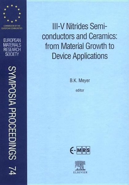
III-V Nitrides Semiconductors and Ceramics: From Material Growth to Device Applications
Aus der Reihe
European Materials Research Society Symposia Proceedings
-
- Englisch ausgewählt
Fr. 242.00
inkl. gesetzl. MwSt.,
Beschreibung
Produktdetails
Einband
Gebundene Ausgabe
Erscheinungsdatum
22.07.1998
Abbildungen
illustrations, (some colour )
Verlag
Elsevier Science & TechnologySeitenzahl
330
Maße (B/H)
20.9/27.9 cm
Gewicht
960 g
Sprache
Englisch
ISBN
978-0-444-20518-6
Gallium Nitride and its alloys with InN and AlN, have recently emerged as important semiconductor materials with application to yellow, green, blue and ultraviolet portions of the spectrum as emitters, detectors and high temperature electronics. LEDs based on wide badgap GaN nitrides exhibit excellent longevity and brightness levels. Combined with red LEDs one can, for the first time, have full colour semiconductor displays.The 4 day symposium was presented at the combined 1997 International Conference on Applied Materials/European Materials Research Society Spring meeting (ICAM'97/E-MRS'97) held in Strasbourg (France) from 16-20 June 1997, provided a forum for active nitride researchers covering the most recent developments in all areas of nitride semiconductors. Sessions focused on the aspects of epitaxial and bulk growth of GaN and its alloys, on optical properties and structural and electrical characterisation, quantum phenomena and light-emitting devices such as LEDs and laser diodes.
Noch keine Bewertungen vorhanden
Verfassen Sie die erste Bewertung zu diesem Artikel
Helfen Sie anderen Kundinnen und Kunden durch Ihre Meinung.